晶片特色:
32-bit lockstep dual-TMS320C28x core at 120 MHz
-
IEEE 754 Floating-Point Unit (FPU)
-
Trigonometric Math Unit (TMU)
-
CRC Engine and Instructions (VCRC)
On-chip memory
-
256KB (128KW) of single bank flash (ECC-protected)
-
36KB (18KW) of RAM (ECC/Parity-protected)
-
Dual-zone security
-
Secure Boot and JTAG Lock
Clock and system control
-
Two internal 10-MHz oscillators
-
Crystal oscillator or external clock input
-
Windowed watchdog timer module
-
Missing clock detection circuitry
-
Dual-clock Comparator (DCC)
1.2-V core, 3.3-V I/O design
-
Internal VREG for 1.2-V generation
-
Brownout reset (BOR) circuit
System peripherals
-
52 individually programmable multiplexed General-Purpose Input/Output (GPIO) pins (11 shared with Analog)
-
10 digital inputs on analog pins
-
Enhanced Peripheral Interrupt Expansion (ePIE)
-
Multiple low-power mode (LPM) support
-
Unique Identification (UID) number
Communications peripherals
-
One Power-Management Bus (PMBus) interface
-
Two Inter-integrated Circuit (I2C) interfaces
-
One Controller Area Network (CAN/DCAN) bus port
-
One Controller Area Network with Flexible Data-Rate (CAN FD/MCAN) bus port
-
One Serial Peripheral Interface (SPI) ports
-
Three UART-compatible Serial Communication Interface (SCI)
-
One UART-compatible Local Interconnect Network (LIN) interfaces
Analog system
-
Two 4-MSPS, 12-bit Analog-to-Digital Converters (ADCs)
-
Up to 21 external channels (11 shared with GPIO)
-
Four integrated Post-Processing Blocks (PPB) per ADC
-
-
One windowed comparator (CMPSS) with 12-bit reference Digital-to-Analog Converters (DACs)
-
Digital glitch filters
-
COMPDACOUT (11 bit)
-
-
Three windowed comparators (CMPSS_LITE) with 9.5-bit effective reference DACs
Enhanced control peripherals
-
14 ePWM channels with four channels that have high-resolution capability (150-ps resolution)
-
Integrated dead-band support
-
Integrated hardware trip zones (TZs)
-
-
Three Enhanced Capture (eCAP) modules
-
Two Enhanced Quadrature Encoder Pulse (eQEP) modules with support for CW/CCW operation modes
-
Embedded Pattern Generator (EPG)
晶片方塊圖:
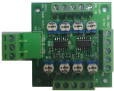
硬體控制卡特色:
-
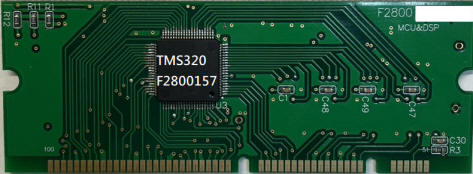
TMS320F2800157數位信號處理器與執行在120MHz,晶片支援浮點運算功能
-
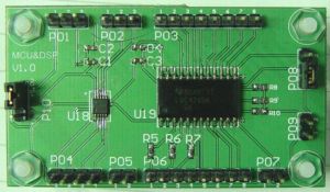
結合USB控制基座(XDS100V2),可插拔式設計
-
USB直接插入電腦,可提供電源
-
支援外接JTAG模擬器,支援程式燒錄等功能
-
支援開機模式設定,可提供最高至1A電流輸出給周邊電路
-
晶片腳位有拉出在USB基座上,包含GPIO、ADC 和其他電源訊號,共計包含41組GPIO腳位與16組ADC腳位(可接受0~3.3V)
-
ADC 通道輸入並包含Anti-aliasing filter (noise filter)功能,可做基本低通濾波電路與電壓保護裝置穩壓
-
依照不同需求可搭配不同基座板進行SCI封包傳輸,可選擇USB基座(USB Adapter)、RS232基座(RS232 Apapter),或搭配無線傳輸設備與模組
發展工具 - 開發環境與軟體:
| 開發環境 | 型號 | 說明 |
|
|
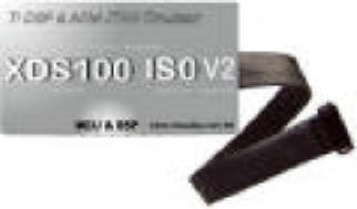
XDS1xx ISO V2(隔離式)模擬器 | 第二代XDS1xx USB介面模擬器,添加隔離式介面,支援CCS4.x、5.x、CCS6.x 。(提供比上一代更高兩倍的傳輸速度)New! |
|
|
最新一代XDS11x USB介面模擬器 ,添加隔離式介面,可支援CCS6.x以上版本。(提供比上一代更高五倍的傳輸速度)New!。 | |
|
|
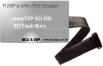
easyDSP-SCI-ISO隔離式SCI傳輸器 | 支援串列訊號TTL轉USB介面,採用隔離式介面 New! |
 |
單極性多功能訊號轉接板 | 提供單極性電壓輸出控制模組,支援標準SPI介面,相容於C2000/MSP430系列所有晶片 |
|
|
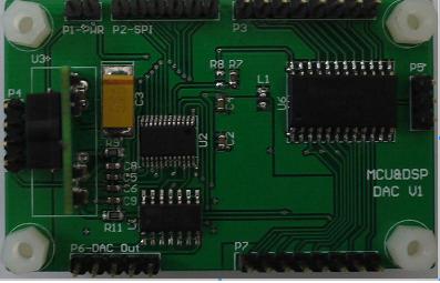
雙極性DAC電壓輸出模組 | 提供正負雙極性電壓輸出控制模組,支援標準SPI介面,相容於C2000/MSP430系列所有晶片 |
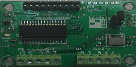 |
兩軸編碼器模組(easyDSP-Encoder) | 兩軸編碼器模組,提供額外32位元QEP解碼電路 。適合在一般IO讀取的環境,相容於C2000/ MSP430/DSP/FPGA系列所有晶片 |
|
|
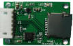
Micro SD儲存裝置(easyDSP-SD Card) | 採用SPI介面資料傳輸,可以相容各式DSP與MCU處理晶片 |
 |
嵌入式DSP系統與CAN匯流排開發套件 | 結合TI DSP處理器的CAN匯流排開發套件 |
 |
4通道降壓轉會模組 | 類比電壓準位轉換模組 |
|
|
4通道升壓轉換模組 | 類比電壓準位轉換模組 |
 |
Code Composer Studio V8.x New! | 最新版軟體開發環境,可支援全系列MSP430/ARM/DSP處理器,可安裝於WIN7/8/10 |