晶片特色:
Dual Core Architecture
-
Two TMS320C28x 32-Bit CPUs
-
200 MHz (5-ns Cycle Time)
-
IEEE 754 Single-Precision Floating-Point Unit (FPU)
-
Trigonometric Math Unit (TMU)
-
Viterbi/Complex Math Unit (VCU-II)
-
16 x 16 and 32 x 32 MAC Operations
-
16 x 16 Dual MAC
-
Three 32-Bit CPU Timers per Core
-
Harvard Bus Architecture
-
Fast Interrupt Response and Processing
-
Unified Memory Programming Model
Two Programmable Control Law Accelerators
-
200 MHz (5-ns Cycle Time)
-
32-Bit Floating-Point Math Accelerator
(IEEE 754 Single Precision) -
Executes Code Independently of Main CPU
On-Chip Memory
-
Up to 1MB Flash, Up to 204KB RAM
-
Boot ROM (64KB)
-
SPI, I2C, CAN, and Parallel I/O Software Boot Modes
-
Standard Math Tables
-
System Peripherals
-
Dual 32- and 16-Bit EMIF With ASRAM and SDRAM Support
-
Dual 6-Channel DMA Controller
-
Up to 169 Individually Programmable, Multiplexed GPIO Pins With Input Filtering
Communications Peripherals
-
USB 2.0 + PHY Port
-
Support for 12-Pin 3.3 V-Compatible Universal Parallel Port (uPP) Interface
-
Two CAN-Bus Ports (32 Mailboxes Each)
-
Three High-Speed (40-MHz) SPI Ports With 16-Level FIFO, DMA Support, and
CLA-Accessible -
Two Multichannel Buffered Serial Ports
-
Four Serial Communications Interfaces
-
Two Inter-Integrated Circuit (I2C) Interfaces
Analog Subsystem
-
Four Dual-Mode Analog-to-Digital Converters
-
16-Bit Mode
-
1.1 MSPS Each (Up to 4.4-MSPS System)
-
Differential
-
External Reference
-
Up to 9 External Channels
-
-
12-Bit Mode
-
3.5 MSPS Each (Up to 14-MSPS System)
-
Single-Ended or Differential
-
External Reference
-
Up to 20 External Channels
-
-
Single Sample-and-Hold (S/H)
(Four-Simultaneous-S/H System) -
Integrated Post-Processing of ADC Conversions
-
Saturating Offset Calibration
-
Error From Setpoint Calculation
-
High, Low, and Zero-Crossing Compare, With Interrupt Capability
-
Trigger-to-Sample Delay Capture
-
-
Analog Comparator/Digital-to-Analog Converter (DAC) Subsystem With Glitch Filter, for Windowed Trip Monitor and PCMC Interfaces
-
Eight Windowed Comparators With 12-Bit DAC References
-
-
Two/Three 12-Bit Buffered DAC Outputs
Enhanced Control Peripherals
-
24 PWM Channels With Enhanced Features
-
16 High-Resolution PWM Channels
-
High-Resolution on Both A and B Channels of 8 PWM Modules
-
Dead-Band Support (on Both Standard and High-Resolution)
-
-
Six Capture Modules
-
Three Quadrature Encoder Pulse (QEP) Modules
-
Two Sigma-Delta Filter Modules (SDFMs) With up to 8 Input Channels, Plus PWM Synchronization
Configurable Logic Block (CLB)
-
Augments existing peripheral capability
-
Supports position manager solutions
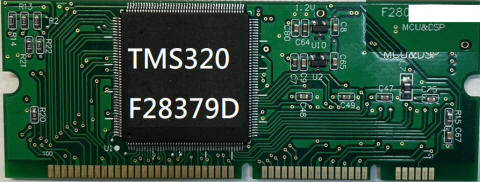
硬體控制卡特色:
-
TMS320F28379D數位信號處理器與執行在200MHz,晶片支援浮點運算功能
-
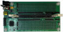
結合USB控制基座(XDS100V2),可插拔式設計
-
USB直接插入電腦,可提供電源
-
支援外接JTAG模擬器,支援程式燒錄等功能
-
支援開機模式設定,可提供最高至1A電流輸出給周邊電路
-
晶片腳位有拉出在USB基座上,包含GPIO、ADC 和其他電源訊號,共計包含44組GPIO腳位與16組ADC腳位(可接受0~3.3V)
-
ADC 通道輸入並包含Anti-aliasing filter (noise filter)功能,可做基本低通濾波電路與電壓保護裝置穩壓
-
依照不同需求可搭配不同基座板進行SCI封包傳輸,可選擇USB基座(USB Adapter)、RS232基座(RS232 Apapter),或搭配無線傳輸設備與模組
發展工具 - 開發環境與軟體:
| 開發環境 | 型號 | 說明 |
|
|
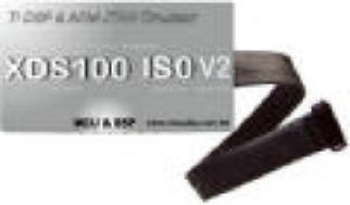
XDS1xx ISO V2(隔離式)模擬器 | 第二代XDS1xx USB介面模擬器,添加隔離式介面,支援CCS4.x、5.x、CCS6.x 。(提供比上一代更高兩倍的傳輸速度)New! |
|
|
最新一代XDS11x USB介面模擬器 ,添加隔離式介面,可支援CCS6.x以上版本。(提供比上一代更高五倍的傳輸速度)New!。 | |
 |
簡易型標準USB控制基座(XDS100V2)與控制卡器專區 New! | 簡易型C2000系列控制卡基座,採用XDS100 V2 USB介面與電腦連接,相容於各式C2000系列控制卡 |
|
|
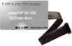
easyDSP-SCI-ISO隔離式SCI傳輸器 | 支援串列訊號TTL轉USB介面,採用隔離式介面 New! |
 |
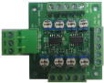
提供單極性電壓輸出控制模組,支援標準SPI介面,相容於C2000/MSP430系列所有晶片 | |
|
|
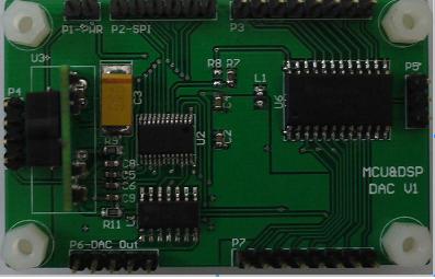
雙極性DAC電壓輸出模組 | 提供正負雙極性電壓輸出控制模組,支援標準SPI介面,相容於C2000/MSP430系列所有晶片 |
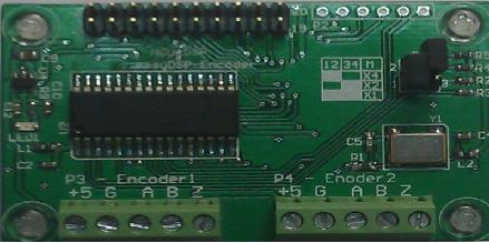 |
兩軸編碼器模組(easyDSP-Encoder) | 兩軸編碼器模組,提供額外32位元QEP解碼電路 。適合在一般IO讀取的環境,相容於C2000/ MSP430/DSP/FPGA系列所有晶片 |
|
|
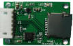
Micro SD儲存裝置(easyDSP-SD Card) | 採用SPI介面資料傳輸,可以相容各式DSP與MCU處理晶片 |
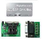 |
嵌入式DSP系統與CAN匯流排開發套件 | 結合TI DSP處理器的CAN匯流排開發套件 |
 |
4通道降壓轉會模組 | 類比電壓準位轉換模組 |
|
|
4通道升壓轉換模組 | 類比電壓準位轉換模組 |
 |
Code Composer Studio V8.x New! | 最新版軟體開發環境,可支援全系列MSP430/ARM/DSP處理器,可安裝於WIN7/8/10 |